Precision Screen Printing Stencil
Total Process Solutions
Delivering highly efficient, precise, and reliable solutions for the industry.
Applications
Delivering precision inspection and imaging solutions for semiconductor, photovoltaic, RFID, PCB, and advanced manufacturing industries.
Semiconductor
Inspection of open/short circuits, copper defects, bubbles, and solder residue on DCB, AMB, and DPC ceramic substrates, plus wire bonding inspection.
Photovoltaic
Quality control of screen meshes for ultra-fine solar cell gridline printing, improving photoelectric conversion efficiency.
High-End Screen Printing
Micron-level defect inspection and fully automatic film-free exposure for RFID antennas and electroformed metal stencils.
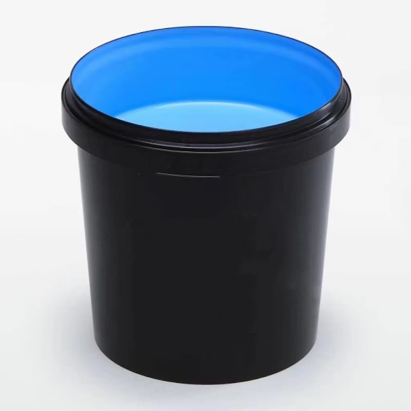
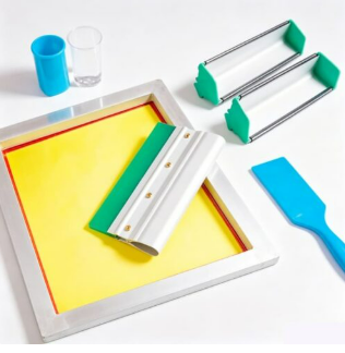
Who is DeepLux?
Suzhou Deeplux Intelligent Technology Co., Ltd. was founded in early 2026, headquartered in Kunshan, China. Our core team has over ten years of experience in screen printing, PCB, semiconductor packaging, photovoltaics, and optical inspection. We are committed to providing “equipment + consumables + process” integrated intelligent manufacturing solutions for global customers.
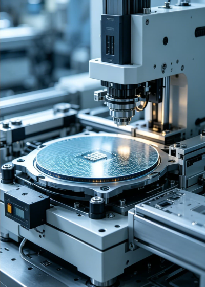
DeepLux in Numbers
3,000+ Sqm
manufacturing facility
10+ Years
Core Team Experience
1.5 µm
Inspection Accuracy
Why Choose Us
Combining advanced hardware, intelligent software, and integrated process expertise to deliver unmatched precision, reliability, and production yield.
Hardware Innovation
Say goodbye to steel-frame deformation. Equipped with aerospace-grade granite bases and magnetic linear motors, our systems deliver ultra-high positioning accuracy of ±1.5 µm.
Software & AI Algorithm
Proprietary GBR-based inspection technology automatically calculates the focal plane without requiring physical samples. Combined with deep learning algorithms, it effectively eliminates false positives and missed defects.
Closed-Loop Ecosystem
We do more than manufacture equipment—we also develop core photosensitive consumables. Through vertical integration of hardware, software, and materials, we deliver fully compatible solutions that maximize production yield.
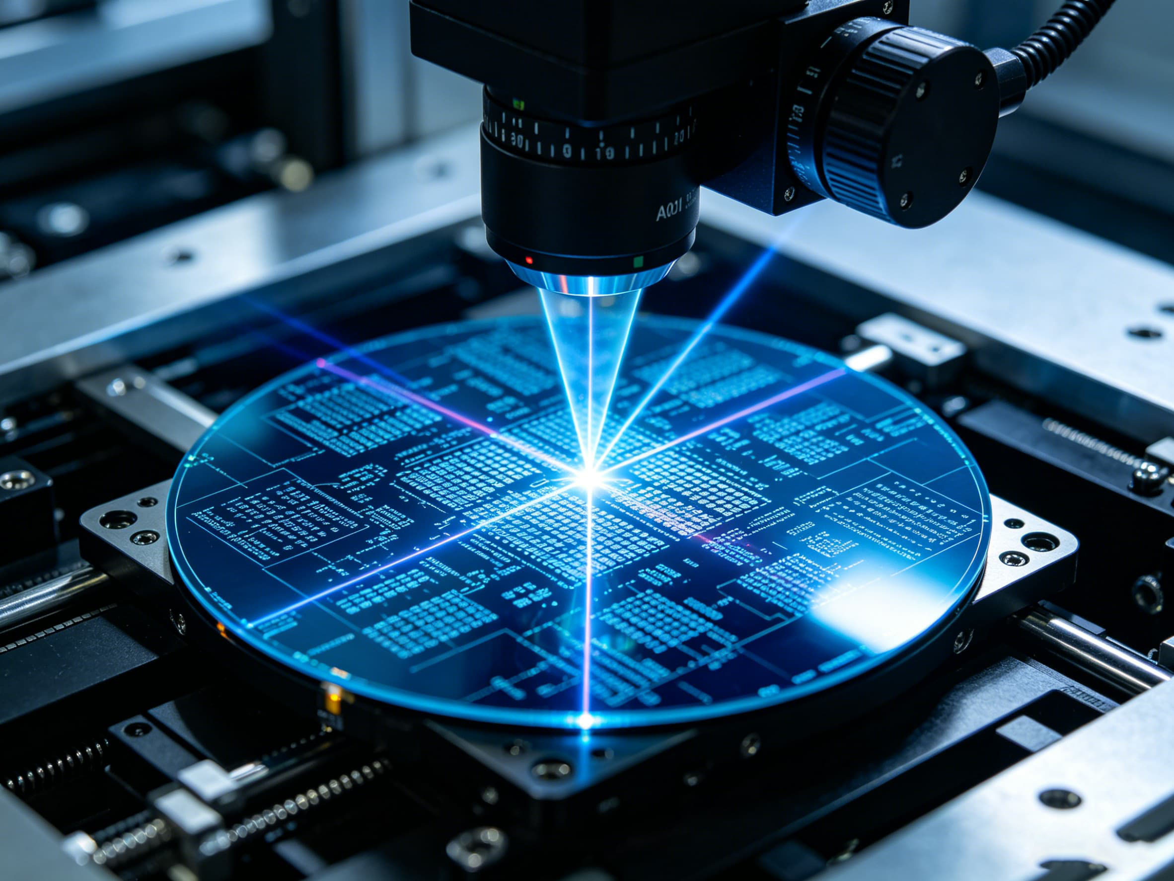
Industry Experience
With over a decade of cumulative industry expertise, our core team has successfully developed and delivered advanced inspection, imaging, and exposure solutions for a wide range of industries, including semiconductors, new energy, 3C electronics, PCB manufacturing, and precision screen printing. Backed by extensive hands-on experience in process optimization and quality control, we help manufacturers improve production efficiency, enhance product reliability, and achieve higher yields through innovative automation and intelligent inspection technologies.
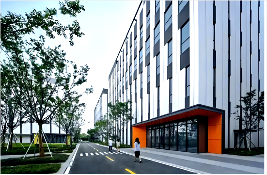
Our Factory
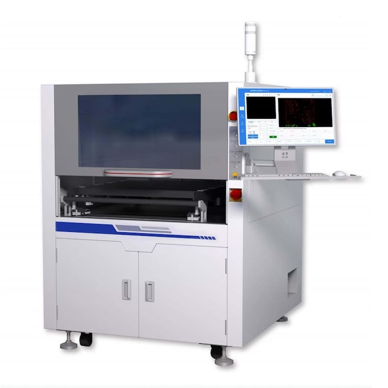
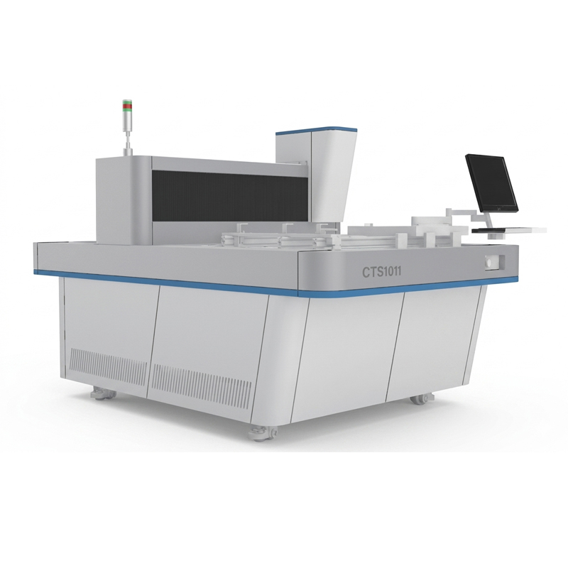
Our manufacturing base in Kunshan covers advanced production lines for direct imaging systems, AOI and coating machines. All equipment undergoes strict calibration and aging tests before delivery.
R&D Capability
300+ Patents & Copyrights
Including 20 invention patents and 1 PCT international patent, demonstrating strong innovation and global competitiveness.
200+ R&D Engineers
A skilled engineering team based in Suzhou, Shenzhen, and Kunshan driving continuous innovation.
Certified R&D & IP Enterprise
Recognized as a Provincial R&D Center and National Intellectual Property Demonstration Enterprise.
Quality Control
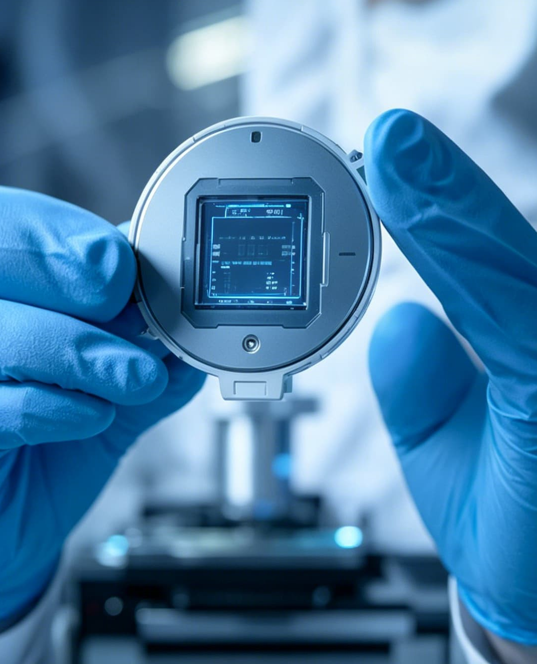
Our production follows ISO9001:2015 quality system. Each machine passes 100% function test, vibration test and continuous operation aging test before packing.
Frequently Asked Questions
What industries and applications are your machines suitable for?
Our Direct Imaging (LDI) systems, AOI inspection equipment, and automatic coating machines are widely used in PCB/FPC manufacturing, semiconductor packaging, photovoltaic (PV) screen printing, and precision screen printing. Feel free to share your specific process requirements – we offer a free preliminary process evaluation and technology selection recommendation.
Do you provide customized equipment or OEM/ODM services?
Yes. We support customization in machine models, software interface, branding, special specifications, and more. For OEM/ODM partnerships, we tailor solutions based on your requirements. Please contact us for detailed customization scope and conditions.
Which international certifications do your products comply with?
Our core products are ISO9001:2015 certified. For export models, we can also support CE, FCC, RoHS, and other international certifications upon request, ensuring compliance with your target market’s regulatory requirements.
What is the minimum order quantity (MOQ)?
Standard machines: 1 unit
Customized machines: subject to negotiation based on configuration
Consumables (emulsions, mesh, etc.): trial orders available upon request
Can I send samples for testing or try a trial run?
Yes. We accept customer samples for free testing and evaluation. You are also welcome to send your actual products to our facility for on-site trial runs. For overseas customers, we can arrange live video participation during the testing process.
What is the typical lead time?
Standard machines: 30–45 working days after deposit receipt
Customized machines: subject to negotiation based on complexity
Rush orders can be accommodated upon discussion
What payment terms do you accept?
We accept T/T wire transfer, L/C, trade guarantees, and other common methods. Standard terms: 60% deposit + 40% balance before shipment. For large orders or long term cooperation, flexible payment arrangements can be discussed.
How are machines packed and shipped?
All machines are packed in export-grade wooden crates, suitable for sea or air freight. We will recommend the best shipping method based on your destination and can also assist with freight and insurance arrangements.
Do you have local agents or service support overseas?
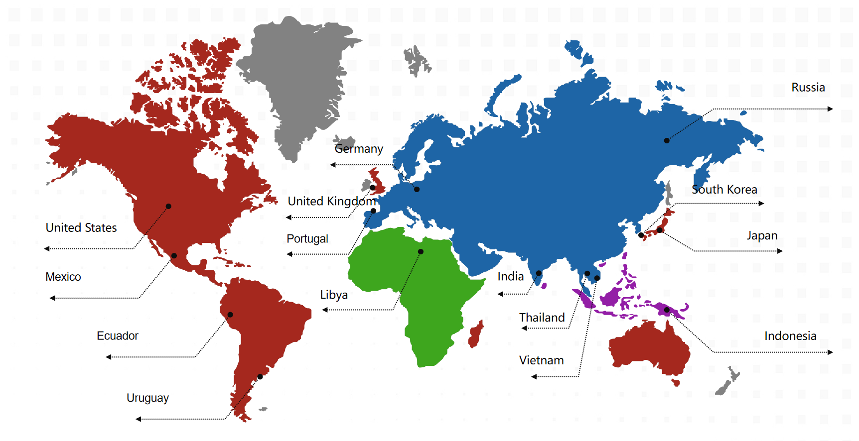
Yes. We have cooperative agents or service partners in many countries and regions, providing local communication and on site support. Contact our sales team to check coverage in your area.
Market